How to NOT design a Yagi-Uda Antenna
So last semester at my telecommunications laboratory I received the task of designing a Yagi-Uda antenna, from the initial design on the jurassic software we used (I know there are other alternatives, but at the time I did not want more trouble, I just wanted to get this project done) all the way to physically building it. It was not easy. I made 3 versions and none of them worked as expected, so today I am going to explain what this type of antenna is, what it is used for, how to properly specify one, and most importantly, what I did wrong during the process. I will also cover an additional test using a Flipper Zero to validate the antenna.
Theoretical Background
Introduction
According to the IEEE Std 145-1983, an antenna can be defined as a device for radiating or receiving radio waves. From that starting point, there are many types of antennas, each with its own characteristics and associated applications.
The Yagi-Uda antenna was invented in 1926 by Shintaro Uda and Hidetsugu Yagi. The central idea consists of a single driven dipole (the active element) placed alongside parasitic elements that are not connected to the transmission line. These parasitic elements receive energy through mutual induction and re-radiate the field, shaping the antenna radiation pattern.
The antenna designed in this project has 3 elements: a reflector, a driven element (dipole), and a director. The reflector is positioned behind the active element and generally has a length slightly greater than lambda/2, typically ranging from 0.50 to 0.53 lambda. The driven dipole, when tuned to resonance, has a length of approximately 0.47 to 0.50 lambda. The director is positioned in front of the driven element and has a length shorter than lambda/2, typically between 0.40 and 0.45 lambda.
When analyzing or developing any antenna, there are general characteristics common to all types that must be taken into account:
- Input Impedance
- Radiation Pattern
- Beamwidth
- Directivity
- Gain
- Bandwidth (BW)
- Front-to-Back Ratio
- Cross-Polarization Discrimination (XPD)
Input Impedance
The input impedance Z_e is the impedance seen at the terminals of the active element, where the transmission line connects to the antenna. For a 3-element Yagi-Uda, this value depends not only on the active dipole but also on the mutual interaction between all elements. Its expression is given by:
\[Z_e = \frac{Z_{11}(Z_{22}Z_{33} - Z_{23}^2) + Z_{12}(2Z_{12}Z_{23} - Z_{12}Z_{33}) - Z_{13}^2 Z_{22}}{Z_{22}Z_{33} - Z_{23}^2}\]where Z_ii are the self-impedances of each element and Z_ij are the mutual impedances between pairs of elements.
Radiation Pattern
The radiation pattern graphically represents how the antenna distributes radiated power in space as a function of direction. For a 3-element Yagi-Uda, the result is a well-defined main lobe concentrated in the direction of the director and a reduced back lobe in the direction of the reflector.
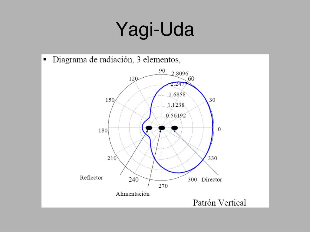
Typical radiation pattern of a 3-element Yagi-Uda antenna. Source: Hali, Antenas, SlideServe, 2014.
Beamwidth
The beamwidth is defined as the angle formed by the points at which the radiated power density falls to half of its maximum value. This angle is defined as the half-power angle.
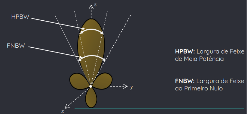
Illustration of the antenna beamwidth (half-power angle). Source: Borges, R. M., Antenas, 2026.
Directivity
Directivity is the ratio between the maximum radiated power density of the antenna and the average power density. In other words, it measures how much the antenna concentrates energy in one direction compared to an isotropic antenna. It is defined as:
\[D = \frac{S_{max}}{S_o}\]where S_max is the maximum radiated power density and S_o is the power density of the reference isotropic antenna.
Gain
Gain expresses the antenna’s ability to concentrate energy in a given direction, taking into account the radiation efficiency. It is calculated as:
\[G_{(dBi)} = 10\log(\eta_I \times D)\]where eta_I = P_i / P_e is the radiation efficiency, P_i is the radiated power, and P_e is the power delivered to the antenna.
Bandwidth
Bandwidth defines the range of frequencies within which the antenna maintains acceptable performance in terms of input impedance and radiation pattern. It is given by the difference between the maximum and minimum operating frequencies:
\[BW = f_{max} - f_{min}\]Front-to-Back Ratio
The front-to-back ratio R_fb is the ratio between the power density at the peak of the main lobe and the power density radiated in the opposite direction. It indicates how well the antenna rejects signals coming from behind:
\[R_{fb}\,(dB) = 10\log\frac{S_{max}}{S_c}\]Cross-Polarization Discrimination (XPD)
Cross-polarization discrimination (XPD) is the ratio, in dB, between the power received in the desired polarization and the power received in the cross polarization. The higher the XPD, the lower the interference between polarizations:
\[XPD\,(dB) = 10\log\frac{P_r}{P_{rx}}\]Antenna Specifications
Considering the target operating frequency of 915 MHz, the wavelength is obtained through the fundamental wave equation:
\[\lambda = \frac{c}{f}\]where:
- lambda is the wavelength (m)
- c is the speed of light in vacuum (approximately 3 x 10^8 m/s)
- f is the operating frequency (915 x 10^6 Hz)
Substituting the project values:
\[\lambda = \frac{300{,}000{,}000}{915{,}000{,}000} \approx 0.328\,\text{m}\quad(328\,\text{mm})\]According to the NBS standard, the length of the active element is typically measured as half a wavelength minus an end-shortening factor to compensate for tip effects, generally resulting in a 5% reduction. For this project, the appropriate length for the driven element is:
\[L_{real} = \frac{\lambda}{2} \cdot 0.95 = \frac{3 \times 10^8}{2 \cdot (915 \times 10^6)} \cdot 0.95 \approx 155.7\,\text{mm}\]where the coefficient 0.95 represents the electrical shortening factor (V_f) adopted to mitigate the tip effect at the conductor ends.
From there, the parasitic element dimensions and spacings can be determined using empirical tables and recommendations from the literature. According to the standard, for short antennas the recommended spacing between the reflector and the driven element, and between the driven element and the director, is approximately 0.2 lambda:
\[d_{re} = d_{ed} = 0.20 \cdot \lambda = 0.20 \cdot 328\,\text{mm} = 65.6\,\text{mm}\]To determine the reflector and director lengths, it is necessary to know the diameter-to-wavelength ratio, which expresses the physical thickness of the metallic element proportionally to the radio wave it will tune. With a conductor diameter of d = 2 mm:
\[\frac{d}{\lambda} = \frac{2\,\text{mm}}{328\,\text{mm}} \approx 0.0061\]Consulting the dimension curves for director and reflector elements (shown below), the recommended lengths for this ratio are approximately 0.484 lambda for the reflector and 0.449 lambda for the director.
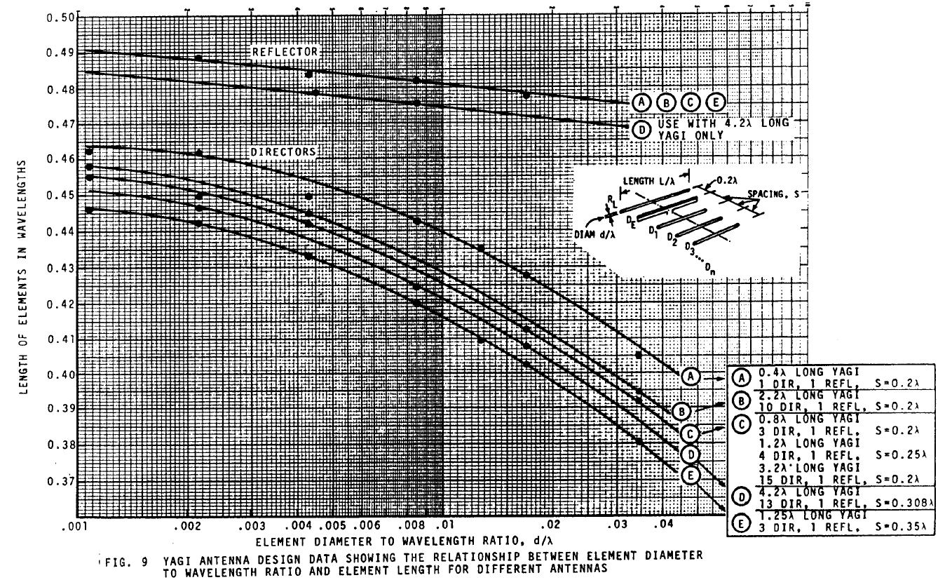
Graph relating the diameter-to-wavelength ratio to the length of the parasitic elements. Source: Viezbicke, P. P., Yagi Antenna Design, NBS Technical Note 688, 1986.
Therefore:
\[L_{reflector} = 0.484 \cdot 328\,\text{mm} \approx 158.7\,\text{mm}\] \[L_{director} = 0.449 \cdot 328\,\text{mm} \approx 147.3\,\text{mm}\]The full set of theoretical dimensions is summarized in the table below.
| Element / Parameter | Proportion Factor | Physical Dimension (mm) |
|---|---|---|
| Reflector (Length) | 0.484 lambda | 158.7 |
| Driven Element (Length) | 0.475 lambda | 157.7 |
| Director 1 (Length) | 0.449 lambda | 147.3 |
| Rear Spacing (d_re) | 0.200 lambda | 65.6 |
| Front Spacing (d_ed) | 0.200 lambda | 65.6 |
Table 1: Theoretical geometric dimensions calculated for the Yagi-Uda antenna.
These values, however, did not yield satisfactory performance in simulation. To address this, several iterations were performed based on the NBS standard, the reference book, and other sources, aiming to achieve input impedance close to 50 ohms and SWR close to 1.0. The final dimensions used for prototyping are shown in the table below.
| Element / Parameter | Proportion Factor | Physical Dimension (mm) |
|---|---|---|
| Reflector (Length) | 0.482 lambda | 158.0 |
| Driven Element (Length) | 0.463 lambda | 152.0 |
| Director 1 (Length) | 0.415 lambda | 136.0 |
| Rear Spacing (d_re) | 0.259 lambda | 85.0 |
| Front Spacing (d_ed) | 0.183 lambda | 60.0 |
Table 2: Adjusted and optimized geometric dimensions for the Yagi-Uda antenna.
Methodology
The methodology followed an iterative prototyping approach with experimental validation, composed of six sequential steps: theoretical review of Yagi-Uda antenna principles; computer simulation in MMANA-GAL with iterative parameter adjustments; manual construction of the prototype with materials available in the laboratory; S11 measurement with the Keysight FieldFox N9923A vector network analyzer; complementary gain tests with RTL-SDR and Flipper Zero; and a comparative analysis between simulated and measured results, identifying the causes of deviations and proposing improvements for future iterations.
The theoretical review involved research through books and online documents covering the operating principles of Yagi-Uda antennas and design parameters such as element lengths, spacings, impedance, and front-to-back ratio for 915 MHz with 3 elements.
In the computer simulation stage using MMANA-GAL, element dimensions and spacings were defined based on theory. The simulation allowed verification of the electrical parameters before physical construction, with iterative adjustment cycles until adequate SWR and impedance values were obtained.
For the physical prototype, the boom was made from wood and MDF, the elements from stainless steel bicycle spokes, the support from PVC pipe, and a coaxial cable was used for the connection. At this stage, constructive limitations were identified, including difficulty in mechanical alignment and the absence of proper soldering.
The measurements were performed with the Keysight FieldFox N9923A vector network analyzer for S11 and bandwidth evaluation.
For complementary validation, an RTL-SDR with GQRX was used for reception and a Flipper Zero as a transmitter at 915 MHz, comparing the signal level received by the Yagi with a simple reference antenna. Finally, the results were analyzed, the main causes of discrepancy between simulated and measured results were identified, and corrective actions were defined for the next prototype iteration.
Additional Tests
Additional tests were performed to validate the second antenna using GQRX, an open-source SDR (Software Defined Radio) application that helps visualize how the signal is received by the RTL-SDR when the Flipper Zero is used as a transmitter. The coaxial cable is connected to the RTL-SDR on one end and wrapped around the driven dipole on the other end. Due to soldering issues, a loss of approximately 3 to 4 dB is expected at this connection.
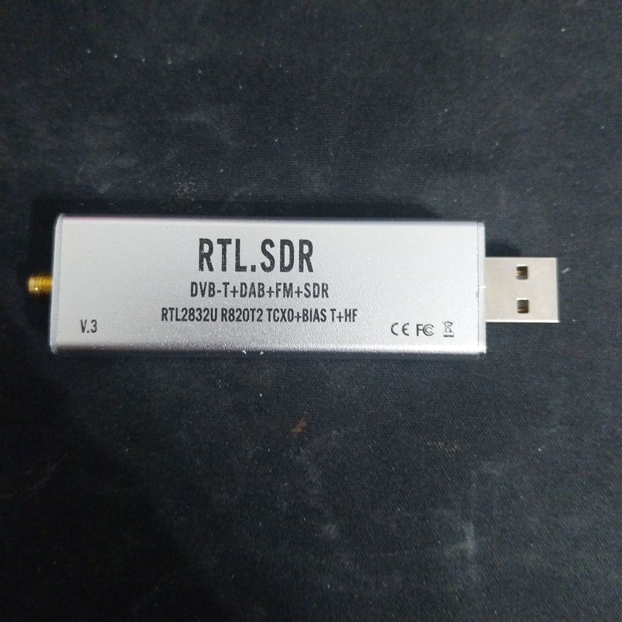
RTL-SDR receiver used in the complementary tests. Source: Author.
For signal transmission, the following procedure was used on the Flipper Zero: select Sub-GHz, then Read Raw, then Config, set the frequency to 915 MHz, record the signal, and then select it for transmission.
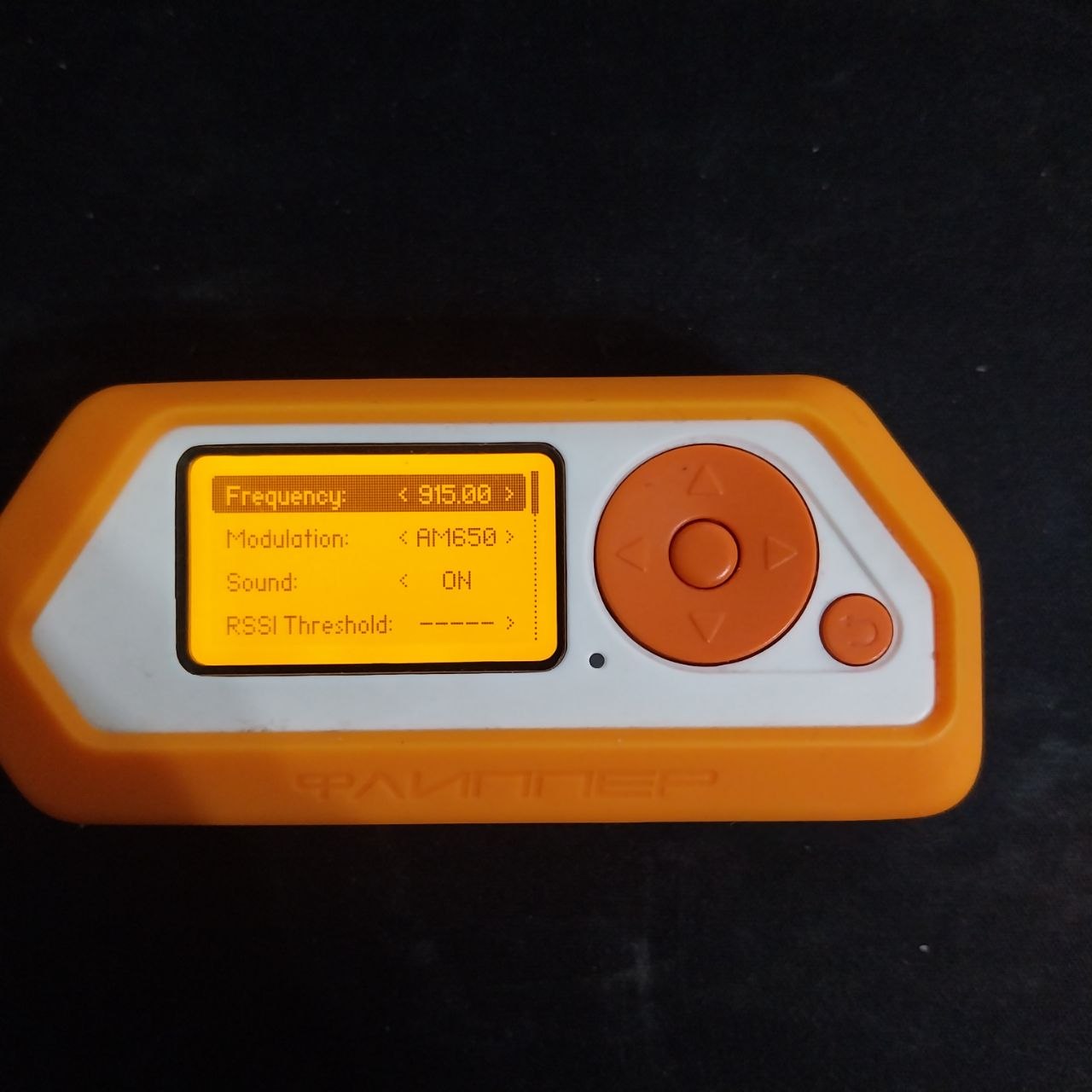
Flipper Zero configuration procedure for signal transmission at 915 MHz. Source: Author.
The dBFS unit refers to the signal level relative to the maximum digitizable value (Full Scale) of an ADC/DAC converter.
When there is no transmission, the dBFS values show the background noise floor of the receiver. In this case, a level of -62 dBFS was observed, which corresponds to thermal and electronic noise, with small variations being natural noise fluctuations.
When the signal is transmitted, the dBFS value shows the signal level relative to full scale. Peaks in dBFS above the noise floor indicate the presence of the signal, and the difference between the signal peak and the noise floor gives the approximate SNR. The signal was found at -47 dBFS over a noise floor of -62 dBFS, giving an SNR of approximately 15 dB.
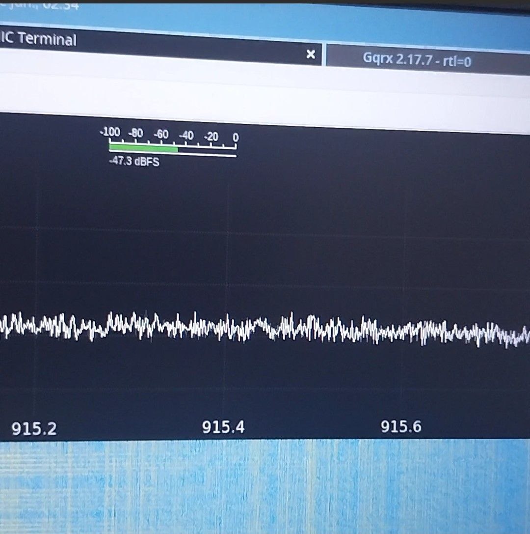
GQRX waterfall and spectrum display during the test. Source: Author.
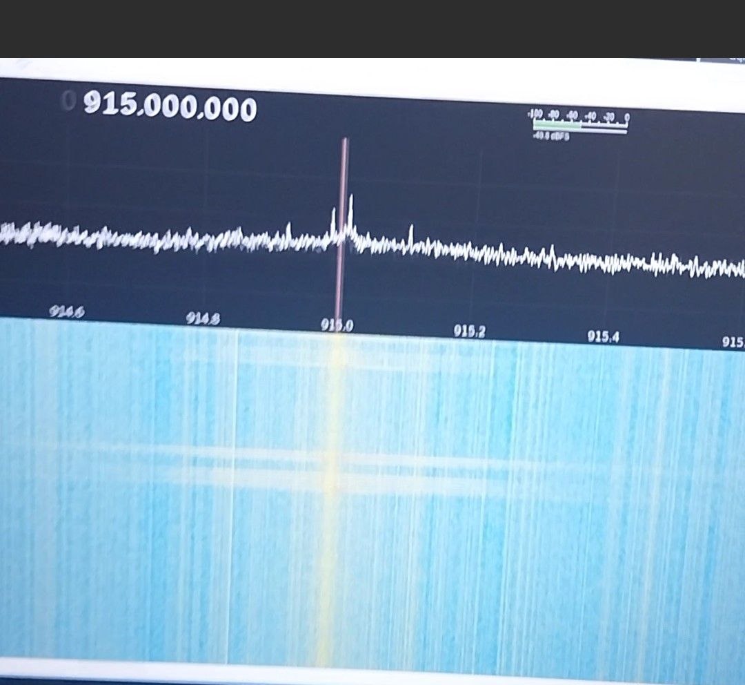
GQRX spectrum detail showing the received signal at 915 MHz. Source: Author.
Results
Simulation Results
In MMANA-GAL, each antenna element was manually entered using its Cartesian start and end coordinates. The conductor radius was set to 1.0 mm for all elements, approximating the diameter of the bicycle spokes used in the physical construction, and segmentation was configured automatically by the software.
Element 1 is the driven dipole, positioned at the origin with a total length of 152 mm. Element 2 is the reflector, displaced 85 mm behind the dipole with a length of 158 mm, slightly longer than the dipole as predicted by Yagi-Uda theory. Element 3 is the director, positioned 60 mm in front of the dipole with a length of 136 mm, shorter than the dipole, also consistent with the theoretical design. All elements lie in the XY plane with Z = 0, characterizing a linear planar antenna.

Element coordinates and dimensions as entered in MMANA-GAL. Source: Author.
The simulation results confirm the expected behavior for a 3-element Yagi-Uda operating at 915 MHz in free space. The main lobe is well defined, with a gain of 7.17 dBi, and the front-to-back ratio of 14.97 dB demonstrates good rejection of signals coming from the rear. The input impedance of 48.81 + j1.56 ohms and SWR of 1.0 indicate that, in the simulated model, the matching with the 50 ohm line is nearly ideal. These results, however, represent an idealized condition, and the deviations observed in the physical measurements reinforce the influence of mechanical imperfections and the absence of a balun on real-world performance.
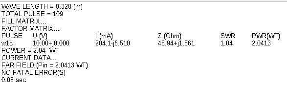
MMANA-GAL Calculate results (No Loss condition). Source: Author.
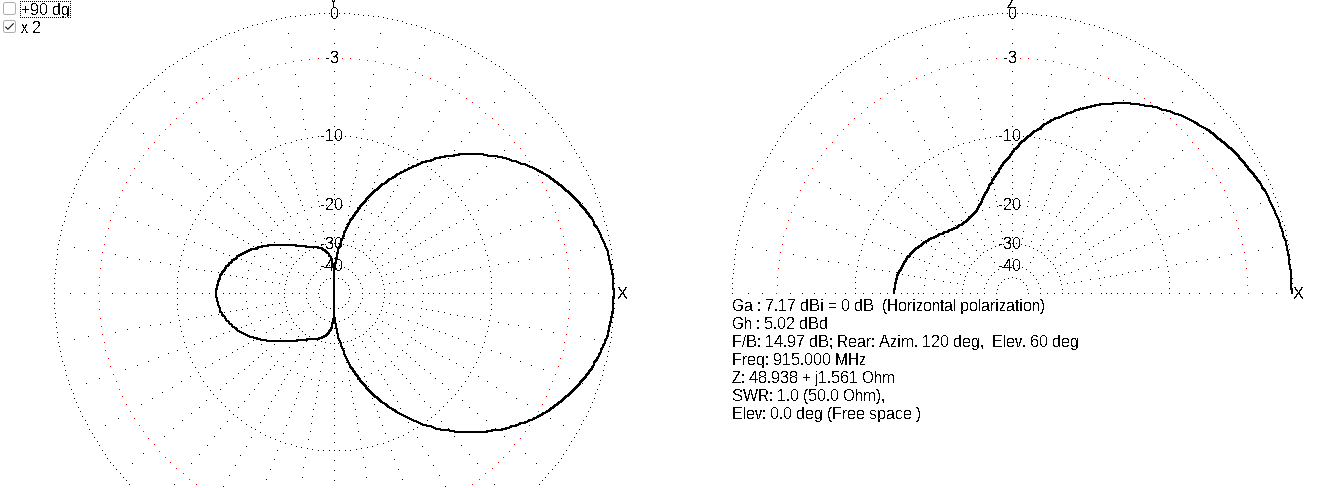
Simulated radiation pattern of the designed Yagi-Uda antenna at 915 MHz. Source: Author.
Measured Results
The Keysight FieldFox RF Vector Network Analyzer was used in the laboratory to verify gain, operating frequency, and S11, which measures the reflection parameter, that is, the amount of signal reflected back at the input port of the device. Three antennas were built, but one of them performed so far below expectations that it will not be covered here.
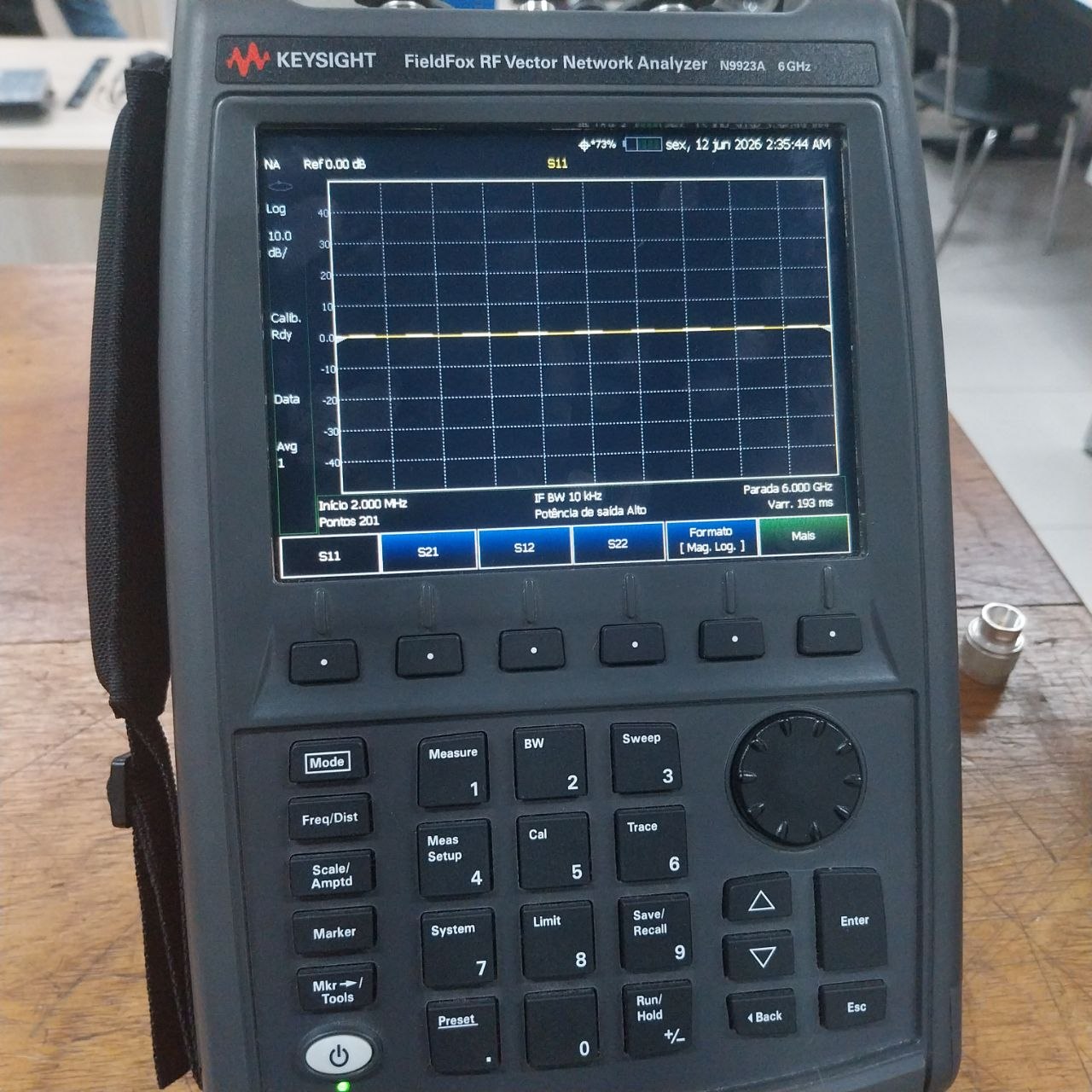
Keysight FieldFox RF Vector Network Analyzer used for measurements. Source: Author.
Antenna 1 resonated at 922 MHz with G = -17 dBi, S11 = -10 dB, and an indeterminate bandwidth. The 7 MHz shift above the target frequency of 915 MHz indicates that the elements are slightly too short, pushing the resonant frequency up. An S11 of -10 dB, while borderline acceptable, reveals insufficient impedance matching between the antenna and the 50 ohm transmission line, likely worsened by the absence of a balun and by the mechanical imperfections of the construction.
The negative gain of -17 dBi indicates that the antenna is radiating with lower efficiency than a half-wave dipole in free space. This can be attributed to connection losses, element misalignment, and the influence of the unbalanced cable on the radiation pattern. The unmeasurable bandwidth further confirms that the matching occurs over an excessively narrow range, making the antenna unsuitable for practical 915 MHz applications without proper dimensional and feed corrections.
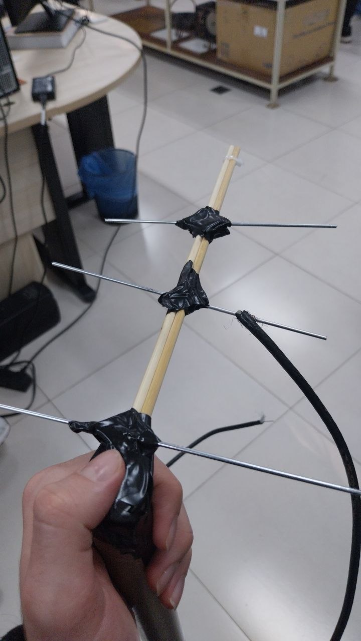
First Yagi-Uda antenna constructed. Source: Author.
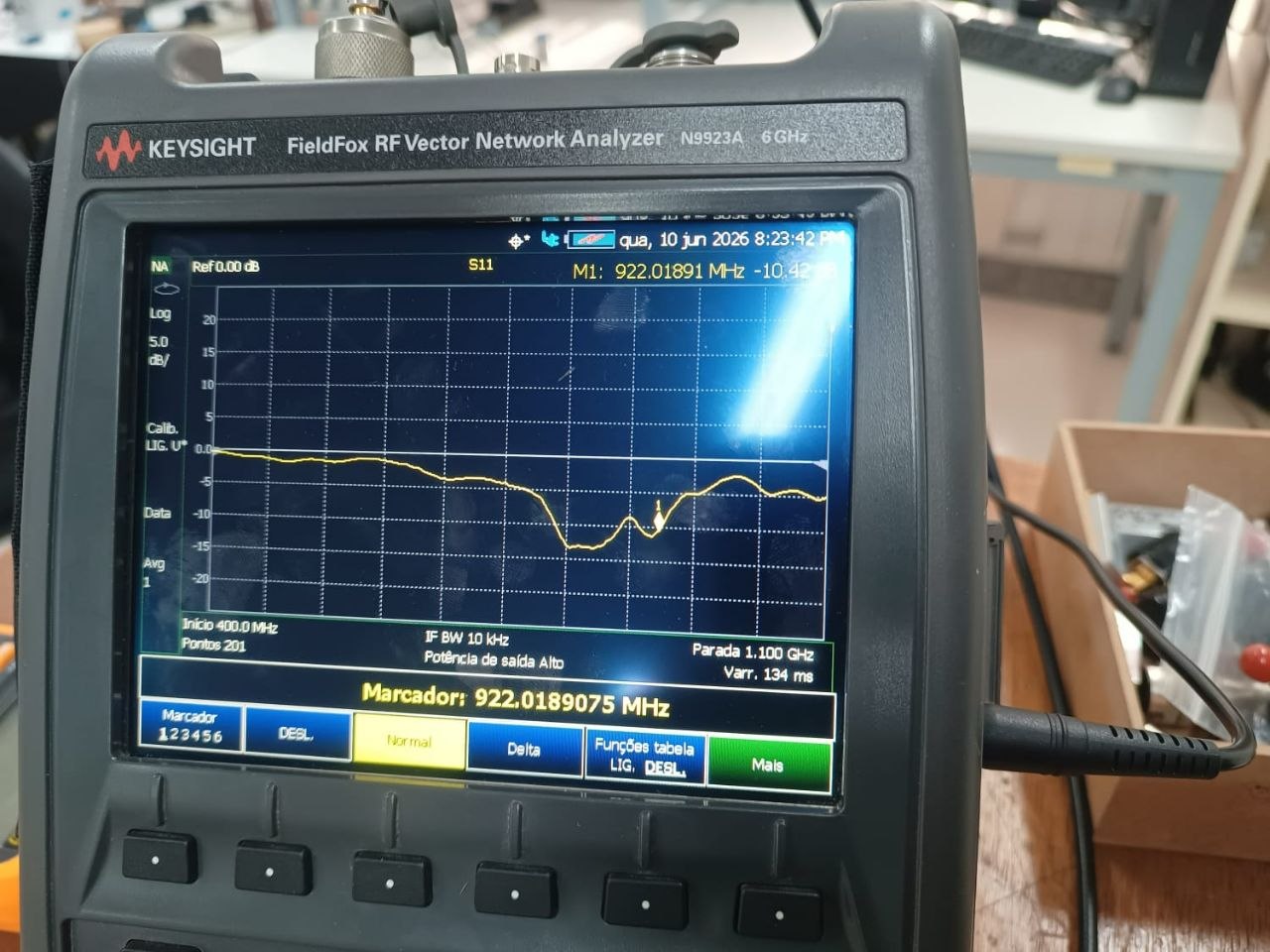
VNA measurement result for Antenna 1. Source: Author.
Antenna 2 maintained S11 close to -10 dB, but the measured resonant frequency shifted significantly to approximately 789 MHz, well below the target of 915 MHz. This downward shift indicates that the elements are electrically longer than specified in the design.
The most likely causes are errors in the physical element lengths, deviations in spacing from the simulated values, and the dielectric effect of the electrical tape used for mechanical fixation, which adds distributed capacitance to the elements and contributes to lowering the resonant frequency. The bandwidth remained zero for the same reason identified in the first antenna, indicating that the mechanical adjustments made were not sufficient to correct the electrical deviations.
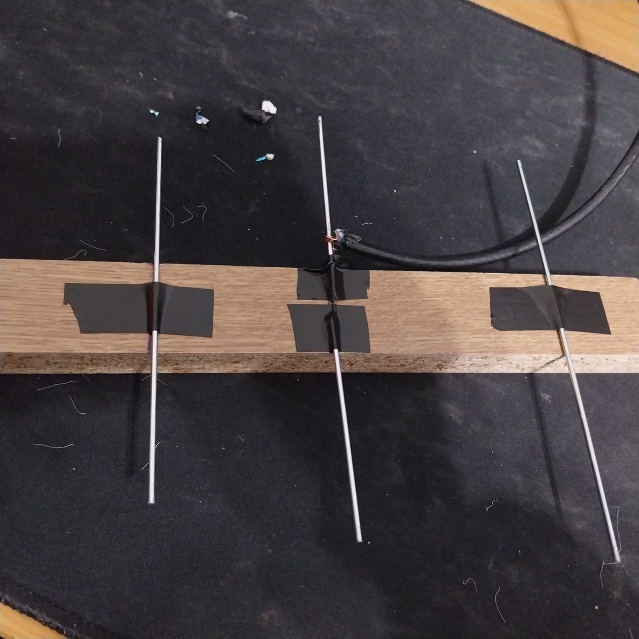
Second Yagi-Uda antenna constructed. Source: Author.
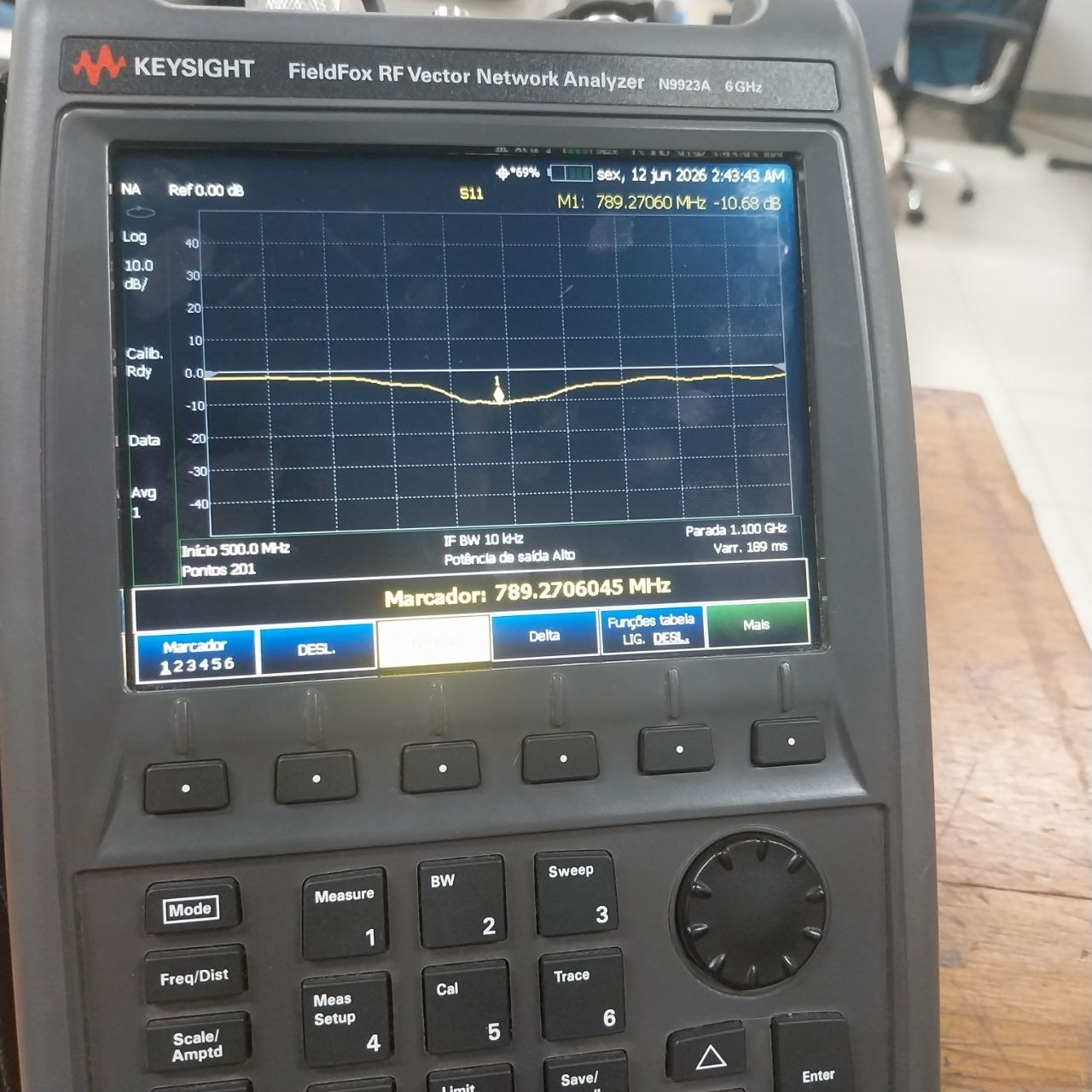
VNA measurement result for Antenna 2. Source: Author.
Analysis
Based on the simulation and laboratory results, it is possible to compare the main reasons why the project did not meet its original specifications.
The first antenna was the one that came closest to the target frequency of 915 MHz, with a measured resonant frequency of approximately 922 MHz. However, its S11 is close to -10 dB, which is at the borderline of acceptable operation. This value would need to be improved for the antenna to work reliably. At a frequency slightly lower than measured, the antenna operates around a similar S11 level but deviates from the 915 MHz target, even if the margin is small.
Another visible issue in the first antenna is its mechanical stability, which directly impacted how the elements behaved. The materials used were not the best choice for meeting the project requirements. Even though the elements were nominally in place, the impact of poor mechanical rigidity was significant.
In the second antenna, the mechanical stability was improved, but the element positioning was still not adequate, resulting in a significant deviation compared to the first result. The main cause is the element arrangement: even though the deviations are within what might seem like a small margin of error, the minimum changes in element length and spacing have a direct and measurable impact on the results. The impedance was also adjusted in an attempt to bring the resistive part closer to 50 ohms and reduce the reactive component.
References
Gqrx SDR, “Gqrx SDR – Open source software defined radio by Alexandru Csete”, Gqrx.dk. Available at: https://www.gqrx.dk/.
Gogolev, M. & Gontcharenko, I., “MMANA-GAL – Antenna Analyzing Software”, GAL-ANA. Available at: https://gal-ana.de/basicmm/en/#18.
Hali, “Antenas”, SlideServe, 2014. Available at: https://www.slideserve.com/hali/antenas.
Ribeiro, J. A. J., Engenharia de Antenas: Fundamentos, Projetos e Aplicacoes. Sao Paulo: Erica, 2004.
Viezbicke, P. P., Yagi Antenna Design, U.S. Department of Commerce, National Bureau of Standards, Washington, DC, USA, NBS Technical Note 688, 1986. Available at: https://tf.nist.gov/general/pdf/451.pdf.